A 4.6: Metallic Nanostructures by Nanocontact Printing and Templating: Antennas and Receivers
Subproject Leader: Thomas Schimmel
Institut für Angewandte Physik, KIT
Contributing Scientists:
Present: Roland Gröger
Past: Sheng Zhong
Motivation
The development of novel photonic and plasmonic devices and technologies such as ultrafast modulators on the basis of silicon, have roused considerable interest recently. In this field, the current world record for the fastest modulator has been achieved within subproject A4.4. While the focus of A4.4 is on devices, their characterization and performance, this subproject A4.6 focuses on the development of the required nanolithographic tools, as well as novel materials and thin films with unusual optical properties.
Recent Results
In the areas mentioned above significant progress was achieved, especially using bottom-up approaches for soft lithography, metal nanowire self-assembly and molecular self-assembly. Recent results include:
-
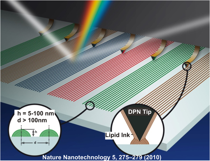
Chemosensitive optical gratings were fabricated on the basis of scanning probe lithography. Dip-Pen Nanolithography was used to produce optical gratings with bio-sensing capability. This novel approach uses the shape change of the liquid crystalline grating upon binding to an analyte, which can be detected in situ by optical means. [1]
-
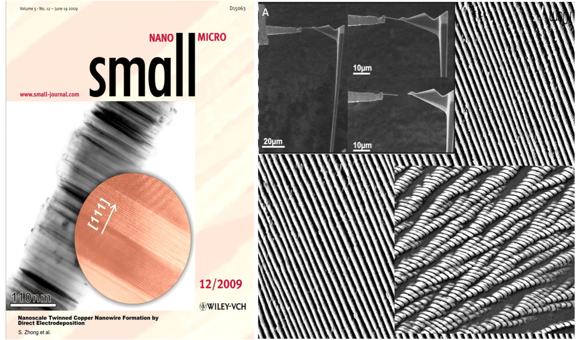
Metallic nanowires made of copper, lead and silver were produced with a variety of tailorable structural properties. With a novel approach based on self-organization, highly regular periodic arrays of mesoscale wires were fabricated – wire arrays to be used as antennas and outcoupling gratings for thin film optoelectronic devices. Furthermore, freestanding wires with an extremely high density of twins were synthesized: a new concept leading to a more than 10-fold higher mechanical strength of the nanowires, compared to normal copper bulk material. [2]
-
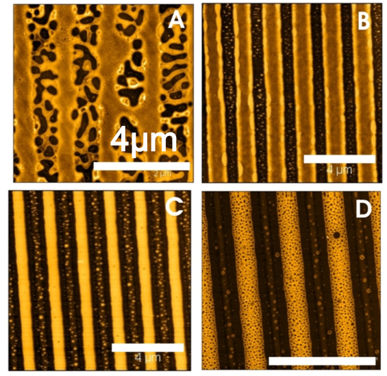
Polymer Templating was used to develop high resolution parallel structuring techniques for metal nanostructures, as required for different CFN projects within Project Area A. The experiments yielded a resolution in the 20-nm range, which is suitable for the production of antenna structures as well as modulators. [3]
-
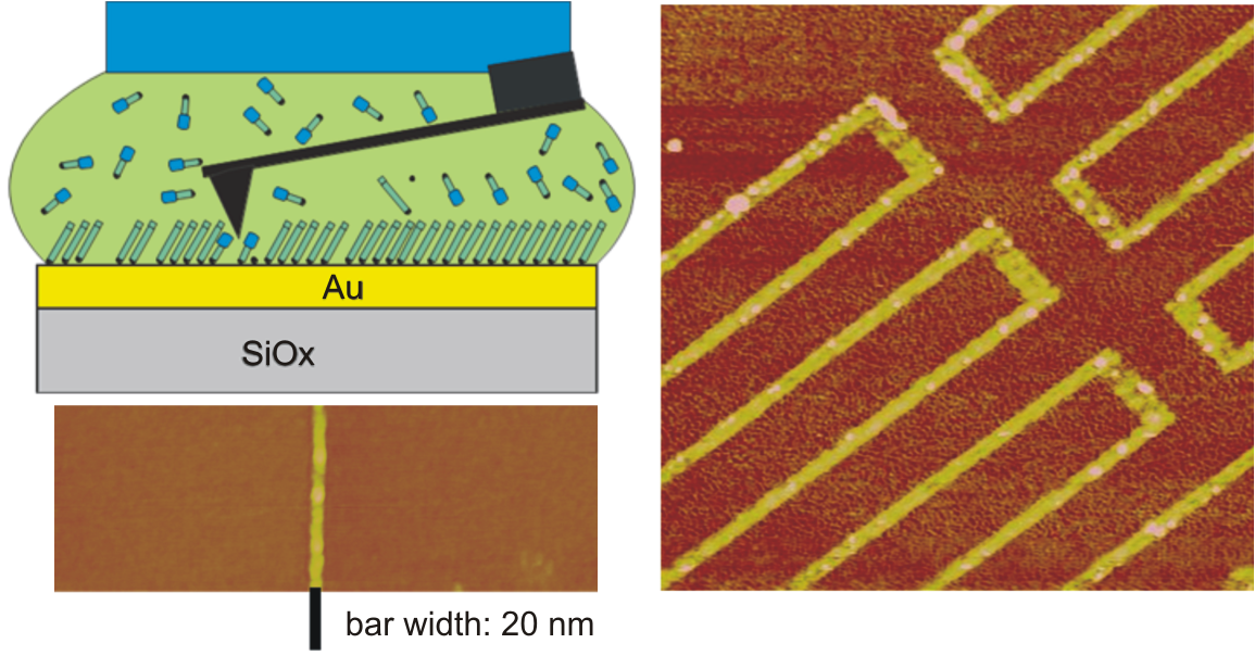
High Aspect Ratio Constructive Nanolithography: polymer brush nanostructures were formed by locally induced constructive nanolithography with a photo-dimerizable moleculewith the tip of an AFM. [4]
In the timeframe 2006-2010 subproject A4.6 (including the preceding project B1.1) has led to 29 publications and 9 patent applications, among which is 1 article in Nature Nanotechnology, 1 in Small, 1 in Advanced Materials and 6 in Langmuir.
References
|
[1] |
S. Lenhert, F. Brinkmann, T. Laue, S. Walheim, Ch. Vannahme, S. Klinkhammer, M. Xu, S. Sekula, T. Mappes, Th. Schimmel, and H. Fuchs: Nature Nanotechnology 5 (4), 275–279 (2010) |
|
[2] |
S. Zhong, Th. Koch, M. Wang, T. Scherer, S. Walheim, H. Hahn, and Th. Schimmel, Small 5, 2265–2270 (2009) Cover Article. |
|
[3] |
T. Geldhauser, S. Walheim, Th. Schimmel, P. Leiderer, and J. Boneberg: Macromolecules, 43 (2), 1124–1128 (2010) |
|
[4] |
M. Barczewski, S. Walheim, T. Heiler, A. Blaszczyk, M. Mayor, and Th. Schimmel: Langmuir, 26 (5), 3623–3628 (2010) |
|
[5] |
Melikyan, N. Lindenmann, S. Walheim, P. M. Leufke, S. Ulrich, J. Ye, P. Vincze, H. Hahn, Th. Schimmel, C. Koos, W. Freude, and J. Leuthold, Optics Express, 19 (9), 8855-8869 (2011) |
List of Publications 2006-2011 as PDF
Subproject Report 2006-2010 as PDF