A4.2: Towards single photon organic semiconductor devices
Subproject Leader: Ulrich Lemmer, Hans-Jürgen Eisler
Light Technology Institute, KIT
Contributing Scientists: Nikola Bralovic, Katja Dopf, Carola Moosmann, Patrick Schwab
Past: Nico Christ, Siegfried Kettlitz, Martin Punke, Sebastian Valouch, Matthias Wissert
Optoelectronic devices based on organic semiconductors are attracting more and more interest for a variety of applications. Large-area organic solar cells and organic light-emitting diodes are in the center of interest. Organic devices can be fabricated by low-cost manufacturing methods based on evaporation or printing/coating on a wide range of different substrates. These include not only traditional substrates for electronics such as silicon or ITO(indium tin oxide)-coated glass but also metal foils or even polymers and paper. Besides the possibilities for large area applications organic semiconductors are very attractive for micro- and nanophotonic devices and systems. The fact that organic semiconductors can be easily patterned opens up new applications in the field of micro-optics [1]. The combination of high speed, organic photodiodes and micro- and nanostructures is promising, as the low process temperatures and the comparably easy fabrication steps necessary to manufacture these devices can be nicely combined with nanopatterning processes and other nanophotonics moieties. Organic semiconductor properties can be significantly modified beyond classic plasmonic enhancement, for example via nanoantennas. Nanoantennas are the scaled down version of conventional radio wave antennas with feature sizes as small as 20 nm, resonant at visible wavelengths. Those metallic nanostructures are specifically designed to efficiently convert free-space radiation from an area larger than their physical dimensions to a localized strongly enhanced field in a confined sub-wavelength dimension by supporting highly localized particle plasmon resonances. Due to their high quantum efficiencies in emission and detection, organic devices combined with those plasmonic nanostructures are very promising for future single photon organic devices.
Fabrication and characterization of gold nanoantennas
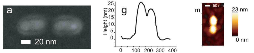
We have successfully fabricated two arm and single arm gold dipole antennas (gap ~20 nm, width ~20 nm, height ~25 nm, variable arm length of 25 nm to 65 nm) using electron beam lithography in cooperation with the group of CFN-member M. Siegel.
A glass cover slip is covered with a 30 nm layer of indium tin oxide (ITO) that serves as a conducting layer for the e-beam step and also helps to provide improved adhesion of the gold on the surface. The e-beam resist PMMA (poly(methylmethacrylate)) is spun onto it and e-beam lithography is performed. After development, a 30 nm gold layer is deposited via thermal evaporation and subsequently a lift-off process is performed resulting in gold nanoantenna structures resonant at optical frequencies.
The topographical properties of the structures are measured with high accuracy by means of atomic force and scanning electron microscopy. Optical measurements are performed using scattering far-field detection via dark-field microscopy. For detection either a single photon avalanche photodiode or a spectrometer with an EMCCD camera can be used.
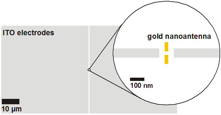
Design concept of future nanostructured organic photodiodes
In accordance with the performed simulations and the comprehensive experimental investigations of the fabricated gold dipole antennas [2-4], an OPD consisting of a single gold dipole nanoantenna, two rectangularly shaped ITO electrodes that are aligned perpendicular to the long antenna axis, organic layers and an encapsulation layer is the most promising design for optical antenna devices. It is an experimental challenge to combine the nanoscale and microscale dimensions of such architecture with high alignment precision. We anticipate to develop those future nanostructured organic photodiodes with nonlinear opto-electronic organics with single photon sensitivity, since we have successfully demonstrated for the first time single photon sources from single colloidal quantum dots at ambient conditions via two-photon laser excitation [5].
|
[1] |
Punke, M.; Valouch, S., Kettlitz, S.W.; Gerken, M.; Lemmer, U.: “Optical data link employing organic light-emitting diodes and organic photodiodes as optoelectronic components,” J. of Lightwave Technol. 26(7), 816-823 (2008) |
|
[2] |
M. D. Wissert, A. Schell, K. S. Ilin, M. Siegel, H.-J. Eisler, Nanoengineering and Characterization of Gold Dipole Nanoantennas with Enhanced Integrated Scattering Properties, Nanotechnology 20, 425203 (2009) |
|
[3] |
M. D. Wissert, K. S. Ilin, M. Siegel, U. Lemmer, H. J. Eisler Coupled nanoantenna plasmon resonance spectra from two-photon laser excitation, Nano Lett. 10, 4161 (2010) |
|
[4] |
M. D. Wissert, C. Moosmann, K. S. Ilin, M. Siegel, U. Lemmer, H.-J. Eisler Gold nanoantenna resonance diagnostics via transversal particle plasmon luminescence Opt. Express 19, 3686--3693 (2011) |
|
[5] |
M. D. Wissert, B. Rudat, U. Lemmer, H.-J. Eisler Quantum dots as single-photon sources: Antibunching via two-photon excitation Phys. Rev. B 83, 113304 (2011) |
List of Publications 2006-2011 as PDF
Subproject Report 2006-2010 as PDF