A2.6: Optimized Quantum Dots for Spin Devices and Optical Resonator Structures
Subproject Leader: Daniel Schaadt
Young Scientist Group - Schaadt, KIT
Contributing Scientists:
Present: Mathieu Helfrich
Past: Yu-Chi Hsu, Dongzhi Hu, Ralf Schuber
The Quantum Effect
Semiconductor devices form the heart of today’s technological progress of our information society. Computers and modern communication technologies which are all based on semiconductor devices play without doubt a fundamental role in our daily life. New semiconductor devices are sought after for various reasons: a huge demand for increased capacities of data storage and transfer, faster and especially secure communication, physical limits of further miniaturization of current devices, to name a few.
When control of the fabrication process of crystalline materials on atomic scale was demonstrated in the late 1960s (molecular beam epitaxy by Arthur and Cho) the road was paved for the development of novel structures with dimensions in the nanometer range. In order to meet with above needs, these nanostructures are exploited with respect to their quantum properties which inevitably emerge due to their reduced size.
In quantum dots electrons (and holes) are spatially confined in all three dimensions. They exhibit atomic-like energy levels and allow for easy access to and manipulation of the confined species and their properties.
Mastering Randomness
Semiconductor quantum dots are conventionally grown in a self-assembly process, the so called Stranski-Krastanov growth mode. This approach is random in nature and if one thinks of scalable applications randomness seems rather inconvenient. That is why researchers have been looking for a way to control the position and size of quantum dots. It was found that small holes on the substrate surface were useful to spatially define nucleation sites where quantum dots would preferentially grow. A large variety of old and new surface patterning techniques was therefore exploited and developed in order to fabricate shallow holes with tens of nanometer dimensions on semiconductor surfaces. Electron beam lithography and wet or dry chemical etching are such powerful techniques which we currently employ to pre-structure GaAs substrates. We then use molecular beam epitaxy to grow site-selective InAs quantum dots. In(Ga)As/GaAs is of particular interest because of its tunability of the bandgap in a technologically interesting range and the long experience with this system.
A Different Control Mechanism
Despite of the successful combination of top-down lithography and bottom-up self-assembled growth, obstacles remain with controlling the quantum dot density, size and shape. One approach to address these problems is to make use of the fact that quantum dots undergo morphological changes during annealing. A better size uniformity was observed after in-situ annealing of quantum dots on un-structured substrates [1]
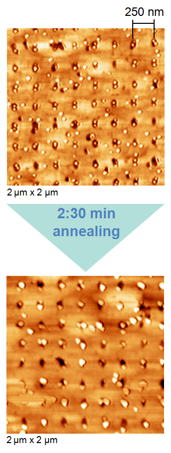
We have recently shown that under specific annealing conditions, original site-selective double-dots merge into single dots [2], see Fig. 1. At the same time, the density of dots nucleating between the pre-defined holes was reduced. We also addressed technological issues with the sample preparation and improved the cleaning procedure before epitaxy [3]. The optical activity of the site-selective quantum dots was statistically confirmed by combining photoluminescence measurements with atomic force microscopy imaging [4].
Supporting Other CFN Efforts
The close relation between this subproject and subproject A2.8 will allow for combination of site-selective quantum dots with optimized micro resonators in order to couple both systems with the prospect of spintronic applications.
|
[1] |
D. Z. Hu, A. Trampert, and D. M. Schaadt, J. Crystal Growth 312, 447 (2010) |
|
[2] |
M. Helfrich, D. Z. Hu, J. Hendrickson, M. Gehl, D. Rülke, R. Gröger, D. Litvinov, S. Linden, M. Wegener, D. Gerthsen, T. Schimmel, M. Hetterich, H. Kalt, G. Khitrova, H. M. Gibbs, and D. M. Schaadt, J. Crystal Growth, in press (2010) |
|
[3] |
M. Helfrich, R. Gröger, A. Förste, D. Litvinov, D. Gerthsen, T. Schimmel, and D. M. Schaadt, Nanoscale Res. Lett. 6, 211 (2011) |
|
[4] |
J. Hendrickson, M. Helfrich, M. Gehl, D. Z. Hu, D. Schaadt, S. Linden, M. Wegener, B. Richards, H. Gibbs, and G. Khitrova, Physica Stat. Solidi C 8(4), 1242 (2011) |
List of Publications 2006-2011 as PDF
Subproject Report 2006-2010 as PDF