A1.4: Three-Dimensional Photonic Crystals
Subproject Leader: Martin Wegener
Institut für Angewandte Physik, KIT
Contributing Scientists:
Present: Isabelle Staude, Joachim Fischer
What is the Excitement About?
To appreciate the excitement about the concept of photonic crystals, it is helpful to stress the analogy to semiconductors for electrons. In a semiconductor, such as, e.g., silicon, the electrons travel as waves through the periodic potential of the nuclei. This leads to Bloch waves with a special dispersion relation, simply the band structure of the solid. For the case of silicon, the band structure has a band gap - the starting point of doping, transistors, computer chips etc. In analogy, light waves moving in a periodic dielectric material can also be described by their band structure. If the parameters are just "right", one also gets a band gap, i.e., a range of frequencies for which propagation is forbidden irrespective of direction, and the photonic crystal becomes a so-called photonic band gap material. This concept was independently introduced by Yablonovitch and John in 1987. Broadly speaking, these "semiconductors for light" smell like fun on the one hand and offer novel options for optical materials of the 21st century on the other hand.
Fabrication Challenges
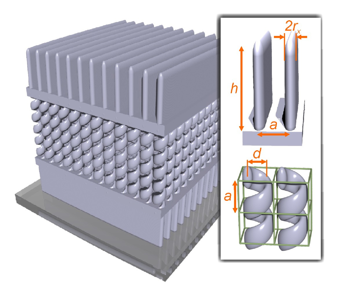
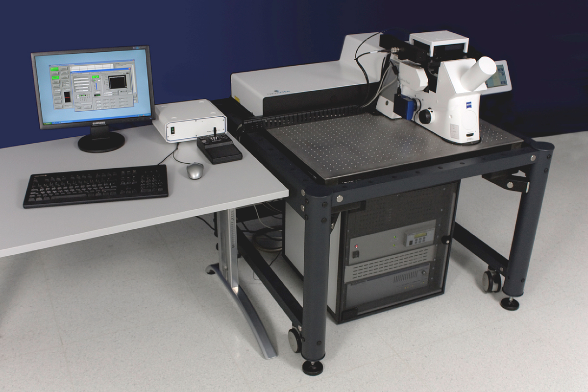
To fabricate such structures, we have developed and optimized a technique called direct laser writing (DLW). In DLW, femtosecond pulses are very tightly focused to a diffraction-limited optical spot. Only in the central region, the light intensity is sufficiently large to lead to significant two-photon absorption. Hence, for a negative-tone photoresist, only this central three-dimensional volume element or "voxel" (in analogy to the two-dimensional pixel element "pixel") remains after the development process. Using computer controlled piezoelectric scanning stages, essentially any arbitrary complex three-dimensional nanostructure can be fabricated along these lines. An early example has been a three-dimensional face-centered-cubic woodpile photonic crystal with a stop band at telecommunication wavelengths [1]. In 2007, we have commercialized the DLW technology via the start-up company Nanoscribe GmbH (see www.nanoscribe.de). Typically, lateral feature sizes as small as 80 nm can be achieved with 800 nm fundamental DLW laser wavelength.
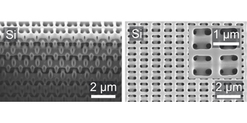
However, to achieve complete three-dimensional photonic band gaps, the refractive index of the photoresist is not sufficiently large. Using a silicon-double-inversion procedure developed in subproject A1.4 in collaboration with chemists (based on silica atomic-layer deposition and silicon chemical-vapor deposition), the polymer structures can be replicated into high-index silicon, leading to complete three-dimensional photonic band gaps at infrared wavelengths [2].
Supporting other CFN Efforts
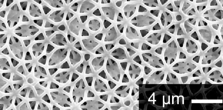
Obviously, DLW allows for fabricating many other interesting photonic structures as well. For example, three-dimensional photonic quasi-crystals [3] or three-dimensional chiral photonic crystals can be made. These and further structures are reviewed in [4,5].
The same DLW technology is also used to fabricate three-dimensional scaffolds for biological cell culture, i.e., "designer Petri dishes" (see subproject E2.3: Behavior of Cells in 2D and 3D Micro- and Nanostructured Substrates) or three-dimensional photonic metamaterials (see subproject A1.5: Photonic Metamaterials) by collaborations within the CFN.
Lately, we have also succeeded to further reduce the accessible lateral and axial minimum feature sizes by combining DLW with ideas inspired by stimulated-emission-depletion (STED) microscopy (also see project E4: Super-Resolution Optical Microscopy) and by developing special home-made photoresists. In principle, arbitrarily small features should become possible along these lines. In practice, designing suitable photoresists in collaboration with CFN chemists poses a major future challenge. This may some day lead to the "holy grail" of the photonic-crystal field, namely to visible-wavelength complete three-dimensional photonic-band-gap materials.
References
List of Publications 2006-2011 as PDF
Subproject Report 2006-2010 as PDF