B1.7: Quantum Coherent Transport in Nanostructures
Subproject Leader: Gerd Schön
Contributing Scientists:
Present: Dmitri Golubev, Fabian Pauly, Alexander Shnirman, Wolfgang Wenzel
Past: Juan-Carlos Cuevas, Robert Maul, Georgo Metalidis, Mickael Pletyukhov, Elsa Prada
Introduction
Electron transport through nanoscale devices shorter than the inelastic mean free path displays the underlying quantum nature of the electrons. Most prominent are interference effects. Another example is the quantization of the conductance through a quantum point contact in units of G0 = 2e2/h arising as consequence of the quantization of electronic states in the constriction. The theoretical description builds on Landauer’s picture viewing electron transport as a scattering problem. Much attention has been devoted recently to spin degrees of freedom in quantum coherent transport, which lead to new effects and allow for further ways of manipulation. Examples are spin transistors, spin valves and spin qubits. The spin-orbit interaction is frequently exploited to couple to the spin, on the other hand, it introduces decoherence. Carbon-based materials, such as nanotubes or graphene could ultimately provide the ideal materials, due to their low spin-orbit coupling and hyperfine interaction. The continuing progress in the fabrication of samples with high mobility and long phase-coherence time makes the field interesting for basic physics as well as device applications.
In the last funding period we studied a number of quantum transport properties, including
- Quantum conductance of electrochemically fabricated point contacts
- Transport properties of graphene heterostructures
- Ballistic electron transport in the presence of spin-orbit interaction
1. Quantum Conductance of Electrochemically Fabricated Point Contacts
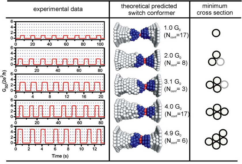
The group of Th. Schimmel (subproject B1.6) succeeded producing switchable nanoscale contacts with predefined quantum conductance by electrochemical deposition techniques. In this process individual metal atoms are exchanged between the electrode and the electrolyte solution, depending on - and controlled by - the applied potential. In view of the microscopic nature of this process, the observed, highly reproducible switching between two different conductance levels, say between zero and five G0, for thousands of cycles, is astonishing. While we can explain the conductance of such junctions on the basis of atomistic calculations [1,2] the physical process underlying the switching remained unclear. Therefore, in parallel to the experimental work we modeled in simulations the principle of the construction and operation of an atomic-scale three-terminal device with predefined quantized conductance [1]. We could explain its mechanism by bistable, self-stabilizing reconstruction of the electrode contact tips at the atomic level.
2. Transport Properties of Graphene Heterostructures
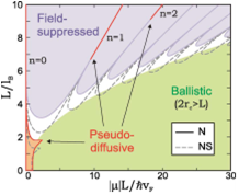
In wide and short (W»L) ballistic graphene samples connected to metallic contacts, it is known that transport at the Dirac point is governed by evanescent modes. Their transmission leads to a universal value of the minimum conductivity at the Dirac point, and surprisingly, to the same transport statistics as in a normal diffusive metal, e.g., a Fano factor of 1/3. We studied the influence of a magnetic field on this so-called pseudo-diffusive behavior, and identified three distinct transport regimes in a magnetic field versus doping phase diagram [3]. We showed how the pseudo-diffusive regime with its typical value of the minimum conductivity is not only present in ballistic graphene, but can also be induced by disorder. We studied the interplay between disorder-induced doping and scattering. We found that the disorder effectively introduces an average potential shift due to doping, and that evanescent modes dominate the transport close to the shifted Dirac point and, at least for short samples (L < W), reinstate a pseudo-diffusive regime. At longer length scales, the system enters a ballistic and then a normal diffusive regime where transport is determined both by the shifted average potential as well as scattering on the individual impurities. Compared with ordinary metals, the presence of adsorbates adds an extra pseudo-diffusive stage to the conventional path towards localization.
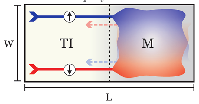
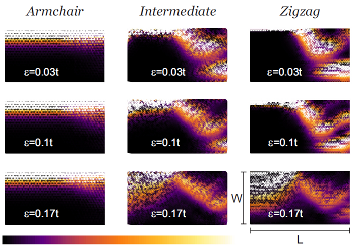
In the presence of intrinsic spin-orbit coupling, a graphene ribbon turns into a topological insulator. This new state of matter is characterized by a bulk energy gap with gapless edge states propagating along the sample edges. In contrast to the quantum Hall effect one finds a pair of counter-propagating spin-up and spin-down states at each edge so that time reversal symmetry is preserved. In Ref. [4], we found that these edge states are transmitted perfectly through a clean junction with a metallic contact. This result is explained by proving the orthogonality between forward- and backscattered edge states analytically. Furthermore, the character of these edge states is fundamentally different for zigzag and armchair edges. E.g., their width only depends on the spin-orbit coupling strength for armchair ribbons, whereas it is practically independent of this parameter for zigzag edge states. In the presence of edge disorder, the perfect transmission is destroyed and the edge states are backscattered when they traverse the sample along the junction interface. However, with increasing ribbon width the perfect transmission is restored as it becomes increasingly difficult to traverse the sample. The topological states are therefore in this sense still protected against backscattering.
3. Ballistic Electron Transport in the Presence of Spin-Orbit Interaction
One of the main goals in the field of spintronics is to develop ways of manipulating an electron's spin with efficiency comparable to that of present-day electronics which manipulates charge. The elementary spintronics device, the so-called Datta-Das transistor, is based on the coherent spin precession in a quantum wire with sufficiently strong Rashba spin-orbit interaction. To fully understand the feasibility of such a device, it is important to investigate the effects of spin-orbit coupling on transport properties of interacting electrons.
We have extended our studies of interaction effects in systems with spin-orbit coupling to the case of two-dimensional electron gas (2DEG). In Ref. [5] we calculated the response functions (charge and spin susceptibilities) of the 2DEG within the Hubbard approximation. We discussed the charge density response to an external magnetic field and the reciprocal effect of the spin density response to an external electric field, which become possible due to the spin-orbit coupling. We observed that in the presence of interaction the enhancement of these effects appears as a result of the excitation of collective charge and spin modes.
Quantum non-local entanglement and current noise seem like two rather distinct phenomena. Somewhat surprisingly, however, the possibility to indirectly diagnose non-local quantum entanglement between quasiparticle spins by current shot noise measurement was recently proposed. The scheme involves cross correlation measurements of shot noise in the output of a beam splitter device built in high mobility heterojunctions. Ideal non-interacting quasiparticles are assumed. The question of whether the proposed scheme is still viable when the spin carriers suffer inelastic scattering was studied. Although inelastic scattering in general destroy quantum correlations, our analysis showed that spin-conserving scattering processes only weakly affect the effectiveness, which still works when quasiparticles have as much as a 50% probability of scattering.
References
|
[1] |
F.-Q. Xie, R. Maul, A. Augenstein, Ch. Obermair, E.B. Starikov, W. Wenzel, G. Schön, and Th. Schimmel, Independently switchable atomic transistors with predefined quantum conductance by reversible contact reconstruction, Nano Lett. 8, 4493 (2008) |
|
[2] |
F.-Q. Xie, F. Hüser, F. Pauly, Ch. Obermair, G. Schön, and Th. Schimmel, Conductance of atomic-sized lead contacts in an electrochemical environment, Phys. Rev. B 82, 075417 (2010) |
|
[3] |
P. San-Jose, E. Prada, and D.S. Golubev, Universal scaling of current fluctuations in disordered graphene, Phys. Rev. B 76, 195445 (2007) |
|
[4] |
G. Metalidis, E. Prada, Transport through a quantum spin Hall insulator – normal junction in graphene nanoribbons, arXiv:1012.4345 |
|
[5] |
M. Pletyukhov and S. Konschuh, Charge and spin density response functions of the clean two-dimensional electron gas with Rashba spin-orbit coupling at finite momenta and frequencies, Eur. Phys. J. B 60, 29 (2007) |
List of Publications 2006-2011 as PDF
Subproject Report 2006-2010 as PDF