B1.4: Preparation and Characterization of Metallic Nanostructures
Subproject Leader: Hilbert v. Löhneysen
Contributing Scientists:
Present: Richard Montbrun
Past: Marc Müller
Making Small Metallic Structures
In subproject B1.4 metallic nanostructures approaching the atomic scale are prepared by various techniques employing “top-down” methods like electron-beam lithography, mechanically controlled break junctions, and nanostructured point contacts through free-standing membranes, as well as “bottom-up” methods like self-organized metallic structures on single-crystalline surfaces. A general focus is to explore the intimate relation between structures and defects in metallic nanostructures on the one hand, and their electronic properties on the other hand.
Structural Correlations on the Quasi One-Dimensional Si(557): Au Surface
Among the one-dimensional (1D) reconstructions induced by submonolayer-thin metals on single-crystalline semiconductor surfaces, the Si(557):Au surface has attracted considerable interest due to its unusual electronic properties found by angular resolved photoelectron spectroscopy. A shift of the position of the upper band from was interpreted as a Peierls-like instability with a mean-field transition temperature Tc = 260 K. A Peierls transition can only occur at finite temperatures in the presence of (albeit weak) additional correlations between the 1D structures. We have shown that structural correlations between the monoatomic chains on the Si(557):Au surface are restricted to one atomic terrace. Apart from the decisive role of the step edge, our results are largely independent of the applied structure model.
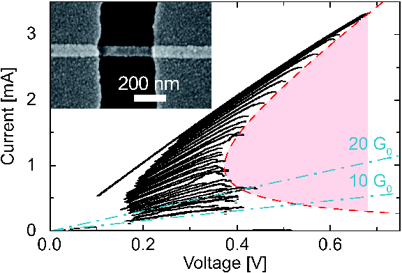
Nanocontacts by Controlled Electromigration
The electronic transport through metallic contacts and wires can be studied down to the single-atom level. Recently it has been shown that electromigration can be used to form electrodes with nanogaps for molecular junctions. A nanowire or nanocontact is heated resistively until thermally activated atoms diffuse under the influence of electromigration forces. Thinning by electromigration works well when the series resistance of the leads is minimized or when a cycling process, intended to limit the power dissipated in the junction, is used. We have recently shown that the latter method yields reproducible results even when nanowires with considerable resistances are used [2].
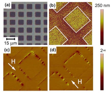
Lateral Modification of Magnetic Order by C-Ion Implantation
Metal-semiconductor compounds such as Mn5Ge3 have been considered as promising candidates due to their easy implementation into the semiconductor-based device fabrication technology. The rather low Curie temperature TC = 304 K of Mn5Ge3 is a severe disadvantage for technological applications. However, the isostructural antiferromagnetic Mn5Si3 can be driven ferromagnetic by insertion of carbon yielding Mn5Si3C0.8 with TC = 350 K. TC is also enhanced in C-doped of Mn5Ge3. Hence, ferromagnetic Mn5Si3Cx and Mn5Ge3Cx could be appealing materials for implementation into semiconductor-based magnetoelectronic devices. We investigated ferromagnetic Mn5Si3C0.8 films prepared by implantation of carbon ions into antiferromagnetic Mn5Si3 sputtered films[3]. Patterning was achieved by using a gold mesh serving as a stencil mask during implantation. MFM images suggest that the ferromagnetic phase is nucleated at the border between the carbon-rich and carbon-devoid Mn–Si phase during implantation at 450 °C. This patterning of initially carbon-free films by ion implantation allows the synthesis of magnetic structures comprised of different magnetic phases. Our work suggests a promising way to obtain lateral magnetic hybrid structures in the micrometer and submicrometer range.
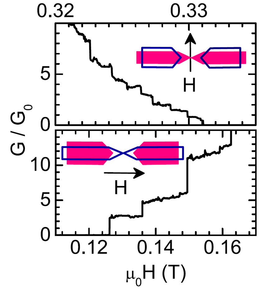
Conductance of Magnetostrictive Nanocontacts
The large magnetostriction (MS) l = 0.003 – 0.008 of the rare-earth metal dysprosium is exploited to tune the conductance G of a break junction by a magnetic field [4]. The field-induced switching for a polycrystalline is observed by the change of the conductance from G0 ≈ 0 to high conductance with increasing field is due to the positive MS of Dy which leads to an elongation of the two electrodes and closure of the contact. In addition to field-induced complete switching between “open” and “closed” states, a step-like behavior of the conductance G(H) with more or less well-defined conductance plateaux can be observed, resembling the behavior of mechanically controlled nanocontacts.
References
|
[1] |
M. Sauter, R. Hoffmann, C. Sürgers, and H. v. Löhneysen, Phys. Rev. B 75, 195436 (2007) |
|
[2] |
R. Hoffmann, D. Weissenberger, J. Hawecker, and D. Stöffler, Appl. Phys. Lett. 93, 043118 (2008) |
|
[3] |
C. Sürgers, N. Joshi, K. Potzger, T. Strache, W. Möller, G. Fischer, and H. v. Löhneysen, Appl. Phys. Lett. 93, 062503 (2008) |
|
[4] |
Marc Müller, Richard Montbrun, Michael Marz, Veronika Fritsch, Christoph Sürgers, Hilbert v. Löhneysen, Nano Letters 11, 574 (2011) |
List of Publications 2006-2011 as PDF
Subproject Report 2006-2010 as PDF