A4.4: Active and Passive Nanowire Waveguides for Optical Signal Processing
Subproject Leader: Juerg Leuthold, Wolfgang Freude
Introduction and Overview
Subproject A4.4. is engaged in next generation active and passive nanowire waveguide structures for integrated optics telecommunications applications. Ultra-compact nanostructured integrated optics devices are envisioned to be key for the development of small form factor transceivers, switches and routers. However, to make them practical a full library of functional components is needed. This library must include lowest loss straight and bent waveguides, passive filters and couplers, active elements such as switches, amplifiers, lasers and detectors. From a practical point of few, it would be desirable if all of these components could be fabricated in silicon and this way take advantage of the vast experience with CMOS technology. In practice, the lack of a direct bandgap prevents a straight-forward fabrication of amplifiers and lasers in silicon. This typically is overcome – either by exploiting Raman amplification in silicon, or by bonding III-V heterostructures onto SOI waveguides. Lastly, the absence of an electro-optic effect makes it difficult to switch at highest speed in silicon.
Novel Silicon Photonics Platform
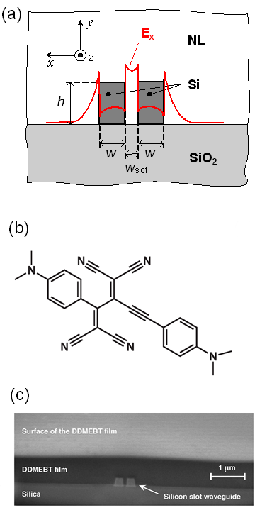
A novel platform to perform optical switching in silicon beyond the current limits has been introduced. This platform relies on the well established silicon-based complementary metal oxide-semiconductor (CMOS) processing technology for fabricating silicon-on-insulator (SOI) waveguides, while an organic cladding layer adds the required nonlinearity [1].
Ultrafast All-Optical Signal Processing
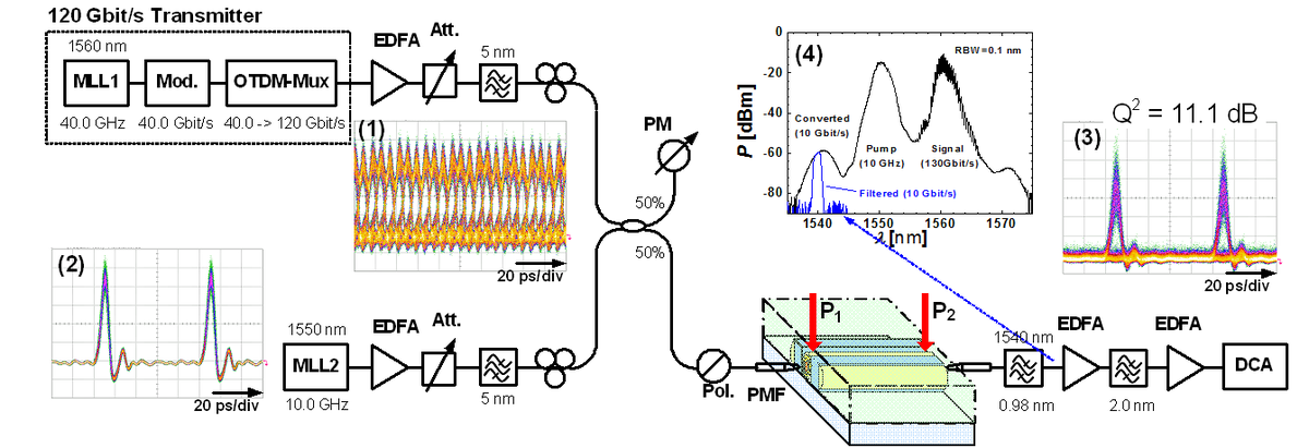
We have already demonstrated 120 and 170 Gb/s [2] silicon signal processing. The theory of which is described in detail in Ref. [3]. The technique so far has been used to demonstrate all-optical demuliplexing [2] and wavelength conversion [4]. It has further been shown, that the new platform does not suffer from any Two-Photon Absorption related Plasma absorption effects that typically lead to speed limitations [3].
Novel Silicon Electro-Optic Modulator
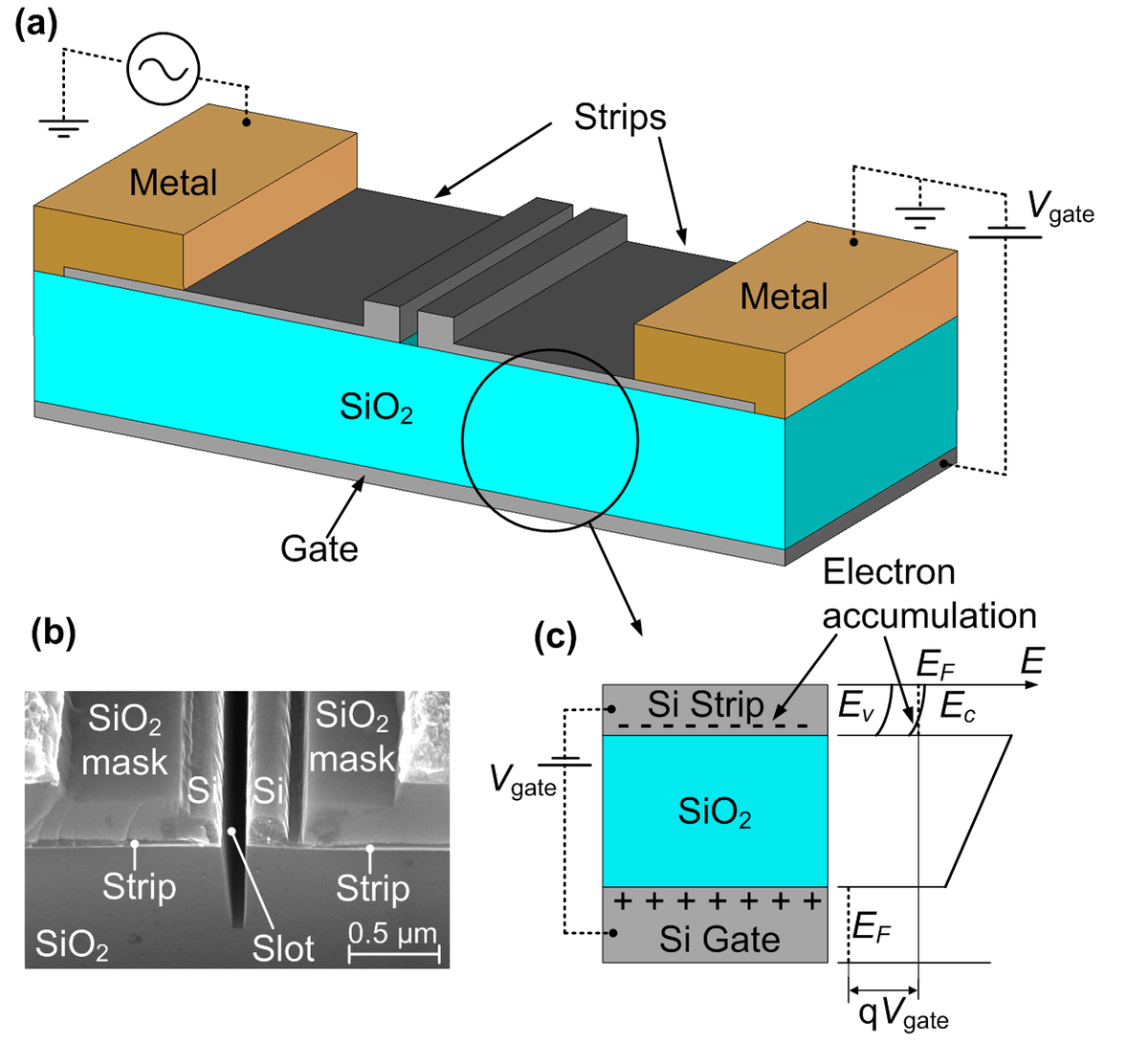
A similar technique relying on the same platform been used to demonstrate 42.7 Gbit/s electro-optic modulators [5]. The phase modulator structures compatible with our SOH approach is depicted in Fig. 3. The phase shifter consist of silicon waveguides (Si) surrounded by a poled electro-optic c(2)-nonlinear organic material [6].
- The SOH allows filling of the slot with a highly nonlinear poled electro-optic material of choice offering almost instantaneous nonlinearity - rather than direct carrier injection in silicon with the related speed limitations.
- The voltage applied across the slotted waveguide electrodes drops off almost entirely across the narrow slot wgap. Since the dimension of the slot is as small as 150 nm one obtains a huge electric field Ex right in the middle of the slot.
- The slotted waveguide structure leads to an optical field almost entirely confined to the slot. These results in an extremely efficient opto-electronic effect since now both the electric and optical fields are largest in the slot.
- The slotted slow-light PhC approach provides an additional field enhancement of the optical field. This enhancement is due to the long time that the optical field resides in the structure and allows to further reduce the length of the phase modulator section.
The SOH platform potentially enables electro-optical modulation with drive voltages around 1 V and bandwidths exceeding 100 Gb/s [6].
Quantum Dot-Semiconductor Optical Amplifiers
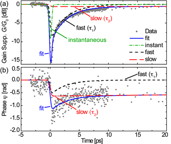
Finally, we have fabricated quantum-dot semiconductor optical amplifiers (QD-SOAs) [7]. For the first time the intricate phase-amplitude behavior has been investigated with a homodyne setup. It was found that the amplitude dynamics is indeed fast – as predicted in literature – yet, the phase dynamics is governed by the dynamics in the wetting layer and therefore shows a relatively slow dynamic [8]. The knowledge about the dynamics has led us to new configurations that enable all-optical wavelength conversion with quantum-dots SOAs. More characterizations have led to insight in the homogenous and inhomogeneous broadening of quantum-dot semiconductor optical amplifiers. The large input power dynamic range has led us to test the suitability for applications with all-optical wavelength converters or applications that need amplifiers for the realization of reach extensions in “extended reach Passive Optical Networks (PON)” [9].
References
| [1] | J. Leuthold1, W. Freude, J.-M. Brosi, R. Baets, P. Dumon, I. Biaggio, M.L. Scimeca, F. Diederich, B. Frank, C. Koos; “Silicon Organic Hybrid Technology A Platform for Practical Nonlinear Optics”, to be published in the Proceedings of the IEEE; (invited) |
| [2] | C. Koos, P. Vorreau, T. Vallaitis, P. Dumon, W. Bogaerts, R. Baets, B. Esembeson, I. Biaggio, T. Michinobu, F. Diederich, W. Freude, and J. Leuthold, All-Optical Signal Processing With Silicon-Organic Hybrid Slot Waveguides, Nature Photon. Vol. 3, pp. 216–219, April 2009 |
| [3] | C. Koos, L. Jacome, C. Poulton, J. Leuthold, and Freude, Nonlinear silicon-on-insulator waveguides for all-optical signal processing, Opt. Express 15, 5976-5990 (2007) |
| [4] | T. Vallaitis, C. Heine, R. Bonk, C. Koos, B. Esembeson, I. Biaggio, T. Michinobu, F. Diederich, P. Dumon, R. Baets, W. Freude, and J. Leuthold, All-Optical Wavelength Conversion at 42.7 Gbit/s in a 4 mm Long Silicon-Organic Hybrid Waveguide, Conference on Optical Fiber Communication 2009 (OFC'2009), submitted |
| [5] | Alloatti, L.; Korn, D.; Palmer R.; Hillerkuss, D.; Li, J.; Barklund, A.; Dinu, R.; Wieland, J.; Fournier, M.; Fedeli, J.; Yu, H.; Bogaerts, W.; Dumon, P.; Baets, R.; Koos, C.; Freude, W.and Leuthold, J.; '42.7 Gbit/s electro-optic modulator in silicon technology'; Optics Express, 19 11841-11851, June 2011 |
| [6] | J.-M. Brosi, Ch. Koos, L. C. Andreani, M. Waldow, J. Leuthold, and Freude, High-speed low-voltage electro-optic modulator with a polymer-infiltrated silicon photonic crystal waveguide, Opt. Express 16, 4177-4191 (2008) |
| [7] | T. Passow, S. Li, P. Feinäugle, T. Vallaitis, J. Leuthold, D. Litvinov, D. Gerthsen, and M. Hetterich, Systematic investigation into the influence of growth conditions on InAs/GaAs quantum dot properties, J. Appl. Phys. 102, 073511 (2007) |
| [8] | Vallaitis T.; Koos C.; Bonk R.; Freude W.; Laemmlin M.; Meuer C.; Bimberg D.; Leuthold J.; 'Slow and fast dynamics of gain and phase in a quantum dot semiconductor optical amplifier'; Opt. Express, Vol. 16, No. 1, pp. 170-178, Jan. 2008 |
| [9] | Bonk R., Vorreau P., Hillerkuss D., Freude W., Zarris G., Simeonidou D., Parmigiani F., Petropoulos P., Weerasuriya R., Ibrahim S., Ellis A. D., Klonidis D., Tomkos I., Leuthold J.; 'An All-Optical Grooming Switch for Interconnecting Access and Metro Ring Networks' Journal of Optical Communications and Networking 3, 206–214, March 2011 |
List of Publications 2006-2011 as PDF
Subproject Report 2006-2010 as PDF