A2.5: Structural and Chemical Properties of Quantum Dot Structures
Subproject Leader: Dagmar Gerthsen
Contributing Scientists:
Present: Holger Blank, Pascal Bockstaller, Dimitri Litvinov, Reinhard Schneider, Roman Walther
Past: Sabine Freidank-Kalhöfer, Nadejda Firman

Electron microscopic techniques are applied in subproject A2.5 to analyze the structural properties and chemical composition of semiconductor nanostructures. Subproject A2.5 has focused on the study of InAs/GaAs quantum-dot (QD) structures which are applied in project A2 in spin-based optoelectronics. Electron microscopy studies are also relevant in context with the new focus of project A2 (since 2009) which is concerned molecular-beam epitaxy (MBE) growth and evaluation of group-III-nitride QDs as spin devices. Another important aspect of subproject A2.5 is the development new imaging and image-evaluation techniques which are required to extract more detailed information on the investigated structures.
InAs/GaAs Quantum-Ddot Structures
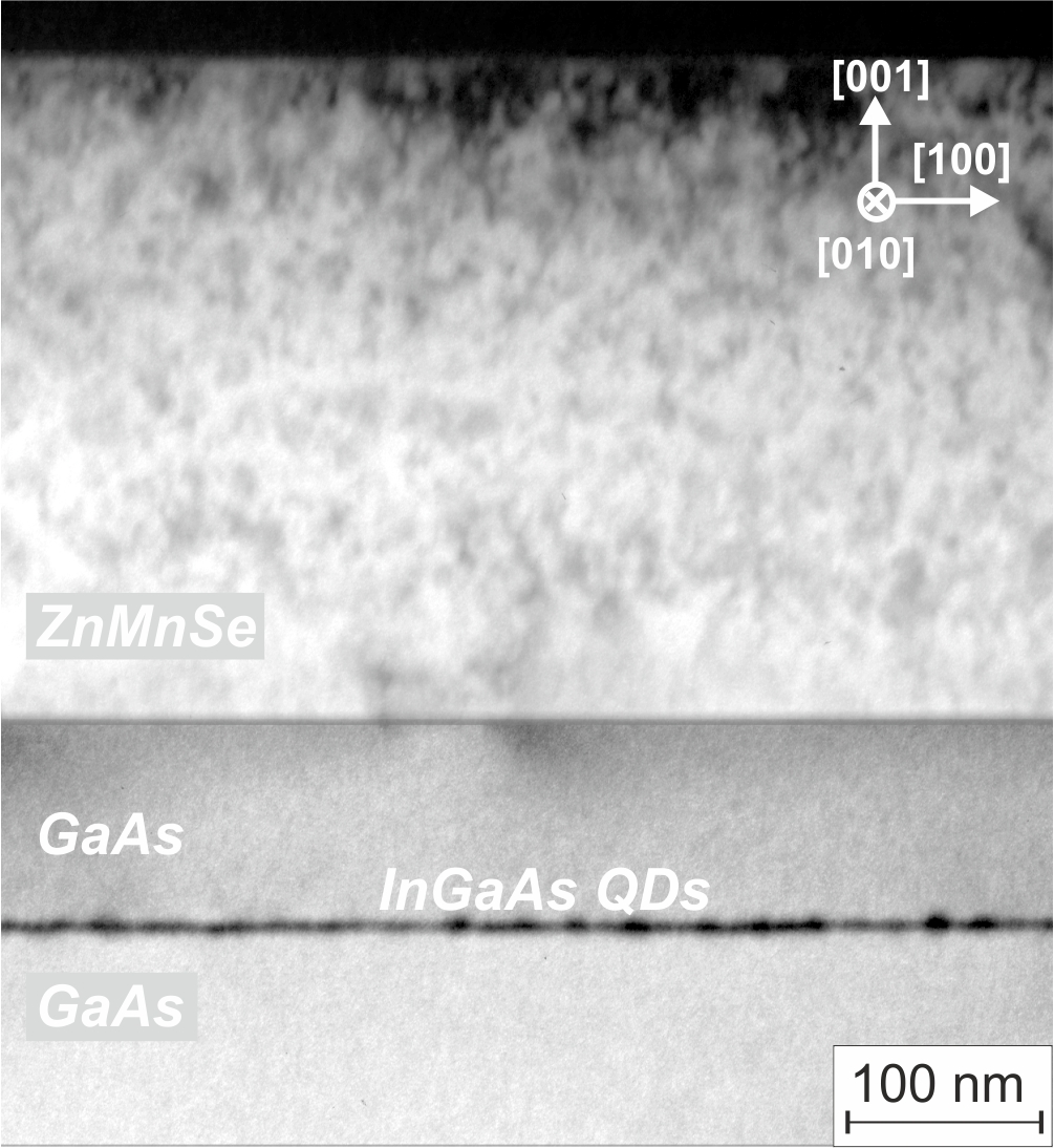
Fig. 1 shows a cross-section TEM image of a spin light-emitting diode which consists of a semimagnetic ZnMnSe spin-aligner layer and InGaAs QDs embedded in GaAs [1].
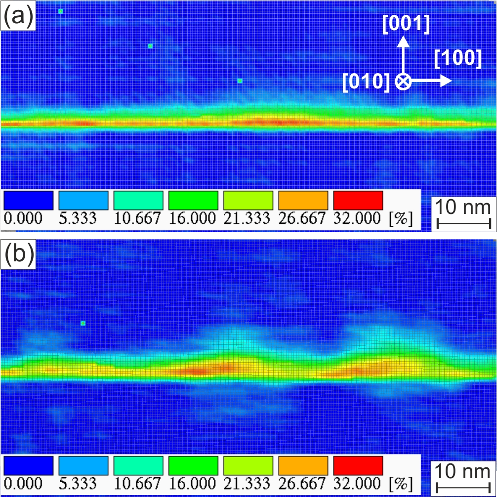
High-resolution (HR)TEM composition analyses based on the composition evaluation by lattice fringe analysis (CELFA) technique show that – among other factors - the QD composition and morphology strongly influences the degree of circular polarization for the electroluminescence. The latter is significantly higher for a quantum-well-type In-distribution (see Fig. 2a) as compared to a pronounced QD morphology (see Fig. 2b).
One important aspect of InAs QD growth is the assessment of the factors which determine the transition between two-dimensional (2D) wetting layer and three-dimensional (3D) island growth which is usually described in terms of a critical amount of deposited InAs. In this context, a study of In-segregation during InAs/GaAs quantum-structure growth was carried out. We demonstrated that a consistent description of the 2D-3D growth mode transition is obtained if a critical amount of segregated indium of 1.1 ± 0.2 monolayers is exceeded in the floating layer on the growth surface [2].
Moreover, a systematic study was carried out regarding the MBE growth of InAs/GaAs QD structures by varying all important growth parameters [3]. This work was motivated by the requirement to identify and understand growth conditions for 1.3 µm QD photoluminescence which is relevant for telecommunication technology. In a separate study the effect of InGaAs cap layers deposited on the QD structure was investigated which leads to a shift of the luminescence towards longer wavelengths and helps to achieve 1.3 µm QD photoluminescence [4].
Further TEM studies were performed on GaAs-based photonic crystal slab nanocavities containing InAs QDs which are attractive for low-threshold lasing and semiconductor quantum optics (collaboration with subprojects A1.4 and A1.5). Fig. 3a shows a cross-section TEM image of a nanocavity with a rough interface between the AlGaAs sacrificial layer and the GaAs on top which is undesirable for cavities with high a quality-factor. The interface quality could be considerably improved (Fig. 3b) by appropriately modifying the MBE deposition conditions [5].
Group-III-Nitride Heterostructures on Si(111) Substrates
Another focus of project A2 since 2009 has been plasma-assisted MBE growth of group-III-nitride heterostructures and their evaluation with respect to spin devices (subproject A2.7). This work is motivated by slow spin dephasing in group-III nitrides possibly even at room temperature. The envisioned spin devices consist of Cu-doped GaN as spin-aligner and InN QDs embedded in GaN or GaN QDs in AlN for spin storage.
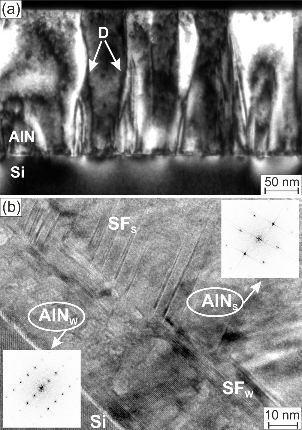
Consequently, a systematic MBE and TEM investigation was carried out regarding the influence of the substrate temperature on the microstructure of AlN and InN layers deposited on Si(111) substrates. The crystalline quality of the AlN and InN layers has to be evaluated with respect to the desired application. For AlN layers, minimum dislocation densities and a smooth surface are obtained for samples grown at 900 °C under Al-rich conditions (see Fig. 4a). However, these samples contain a significant fraction of sphalerite inclusions and stacking faults which are not present at low growth temperatures (see Fig. 4b).
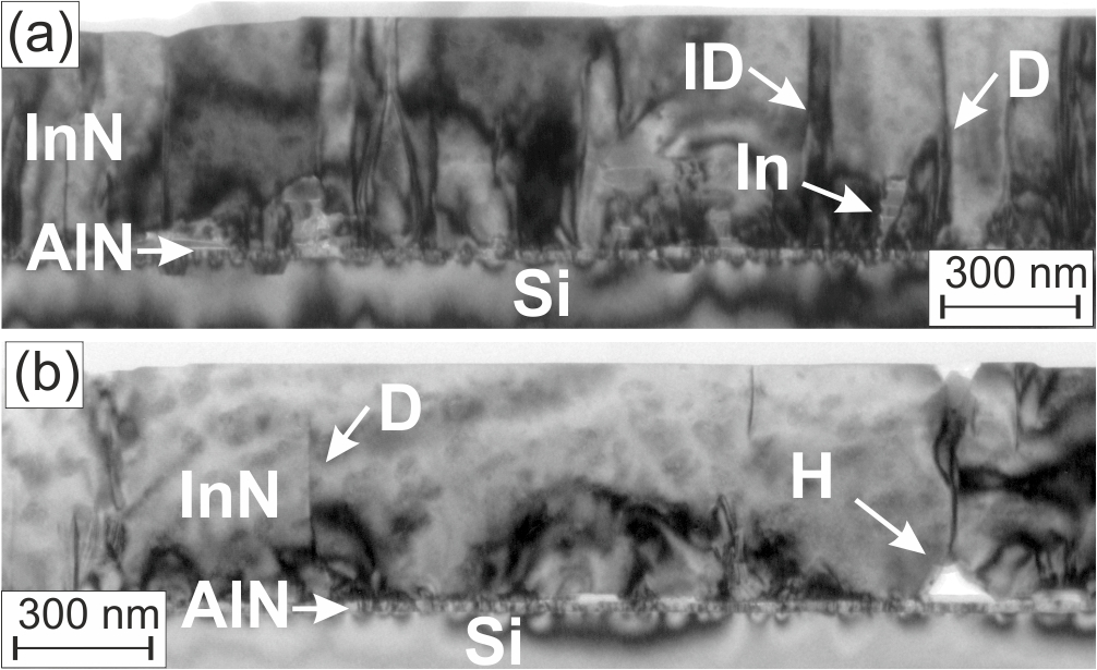
A similar study was performed for InN layers which were deposited on Si(111) substrates and a thin AlN buffer layer at substrate temperatures between 325 °C and 375 °C. Fig. 5 visualizes the complex microstructure of the InN layers which contain not only defects like dislocations (D in Fig. 5), stacking faults and inversion domain boundaries (ID) but also inclusions of indium (In) and indium oxide. At increasing substrate temperature holes (H) are formed close to the AlN/InN-interface (see Fig. 5b).
References
|
[1] |
W. Löffler, D. Tröndle, J. Fallert, H. Kalt, D. Litvinov, D. Gerthsen, J. Lupaca-Schomber, T. Passow, B. Daniel, J. Kvietkova, M. Grün, C. Klingshirn, and M. Hetterich, Electrical spin injection from ZnMnSe into InGaAs quantum wells and quantum dots, Appl. Phys. Lett. 88, 062105 (2006) |
|
[2] |
D. Litvinov, D. Gerthsen, A. Rosenauer, M. Schowalter, T. Passow, and M. Hetterich, Transmission electron microscopy investigation of segregation and critical floating-layer content of indium for island formation in InGaAs, Phys. Rev. B 74, 165306 (2006) |
|
[3] |
T. Passow, S. Li, P. Feinäugle, Th. Vallaitis, J. Leuthold, D. Litvinov, D. Gerthsen, and M. Hetterich, Systematic investigation of the influence of growth conditions on InAs/GaAs quantum dot properties, J. Appl. Phys. 102, 073511 (2007) |
|
[4] |
D. Litvinov, H. Blank, R. Schneider, D. Gerthsen, T. Vallaitis, J. Leuthold, T. Passow, A. Grau, H. Kalt, C. Klingshirn, and M. Hetterich, Influence of InGaAs cap layers with different In-concentration on the properties of InGaAs quantum dots, J. Appl. Phys. 103, 083532 (2008) |
|
[5] |
J. Sweet, B. C. Richards, J. D. Olitzky, J. Hendrickson, G. Khitrova, H. M. Gibbs, D. Litvinov, D. Gerthsen, D. Z. Hu, D. M. Schaadt, M. Wegener, U. Khankhoje, and A. Scherer, GaAs photonic crystal slab nanocavities: Growth, fabrication, and photon storage time, Photonics and Nanostructures 8, 1 (2010) |
List of Publications 2006-2011 as PDF
Subproject Report 2006-2010 as PDF