F1.2: Electronic and Morphological Properties of Organic and Hybrid Solar Cells
Subproject Leader:
Dagmar Gerthsen
Laboratorium für Elektronenmikroskopie, KIT
Uli Lemmer
Lichttechnisches Institut, KIT
Contributing Scientists: Alexander Colsmann, Jens Czolk, Simon Hettler, Michael F. G. Klein, Erich Müller, Philipp Müller, Marina Pfaff, Manuel Reinhard, Sebastian Valouch
Nanomorphology is the Key to High Performance
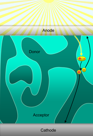
Due to their potential for low-cost photovoltaic applications, organic solar cells comprising polymer/fullerene blends for light harvesting (e.g. P3HT:PC BM and P3HS:PCBM bulk-heterojunctions, figure 1) have attracted a lot of attention over the last decade. Today, it is well accepted that the bulk-heterojunction nanomorphology is a crucial parameter for the fabrication of highly efficient organic solar cells. Thus the thorough investigation of the absorber nanomorphology is of vital importance for further improvements.
Low-Energy HAADF STEM
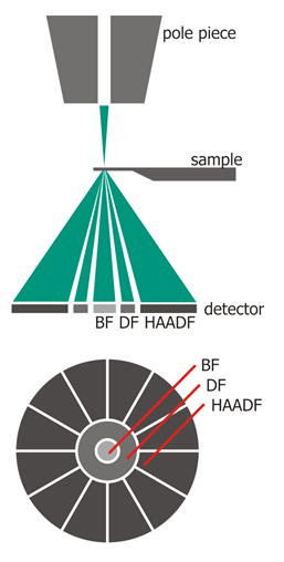
In contrast to the commonly used atomic force microscopy (AFM) and transmission electron microscopy (TEM), we apply scanning transmission electron microscopy (STEM) in a standard scanning electron microscope at electron energies ≤ 30 keV (figure 2). AFM imaging is restricted to monitoring the surface of the sample. TEM imaging is hampered by limitations such as electron knock-on damage, complex mechanisms contributing to image formation and in particular by low contrast for samples containing materials comprising light elements.
Strong chemical contrast (Z-contrast) between sample regions with only slightly different average atomic number and density, like PCBM and P3HS, can be achieved by STEM imaging using a high-angle annular dark-field (HAADF) STEM detector. HAADF STEM imaging is particularly composition sensitive at low electron energies ≤ 15 keV.
To obtain a fundamental understanding of HAADF STEM image formation, we performed a basic study of low-energy HAADF STEM imaging. Monte-Carlo simulations were performed for low density materials (amorphous carbon, P3HS and EPON) and compared with experimental images. It was found that screened Rutherford and Mott electron scattering cross-sections are in general not well suited to describe electron scattering at energies ≤ 15 keV. Therefore, we developed a semi-empirical description to model the HAADF STEM intensity of low-density material [1].
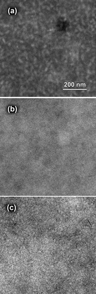
Figure 3 illustrates the advantages of low-energy HAADF STEM in comparison to TEM [2]. The HAADF STEM image in figure 3a clearly shows the shape and size of the P3HS domains with bright contrast. The in-focus bright-field TEM image (figure 3b) of the same P3HS:PCBM layer shows only intensity variations on a coarser scale which are induced by thickness fluctuations of the layer. Strong defocusing is necessary to reveal further contrast features as shown figure 3c. However, defocusing leads to a significant degradation of resolution and a clear interpretation of the image and precise size measurements are not possible anymore.
Correlating Optoelectronic Device Performance and Nanomorphology
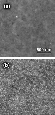
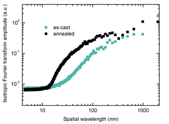
Low-energy HAADF STEM was used to study the influence of the processing conditions and to correlate the changes in the structure of the nanomorphology with the optoelectronic properties of the respective devices. Thermal postproduction treatment of P3HS:PCBM organic solar cells improved the power conversion efficiency by a factor of seven. Simultaneously the nanomorphology changed clearly as visualized by low-energy HAADF STEM, figure 4.
In terms of structure or domain sizes we quantitatively interpret the STEM images by applying a spatial Fourier transform to the STEM images, figure 5 [2].
Further publications of our group cover the influence of the drying kinetics [3], the drying-temperature [4] and the blend composition ratio [5] on the structural evolution of BHJs.
The project is further embedded into research activities on novel organic solar cells in collaboration with industry partners (Merck, Konarka, Cynora, InnovationLab Heidelberg GmbH), with other research collaborations (DFG-priority program 1355 “elementary processes of organic photovoltaics”, P3HS was provided by Merck within the BMBF funded project EOS) and with other research institutions (University of Queensland - Brisbane, bio21 institute - Melbourne, FhG-IAP - Potsdam, Kekulé Institut –Bonn, Physikalisch-Technische Bundesanstalt (PTB) - Braunschweig).
References
| [1] | M. Pfaff, E. Müller, M. F. G. Klein, A. Colsmann, U. Lemmer, V. Krzyzanek, R. Reichelt, D. Gerthsen, Low-energy electron scattering in carbon-based materials analyzed by scanning transmission electron microscopy and its application to sample thickness determination, Journal of Microscopy 243, 31-39 (2011) |
| [2] | M. F. G. Klein, M. Pfaff, E. Müller, J. Czolk, M. Reinhard, S. Valouch, U. Lemmer, A. Colsmann, D. Gerthsen, Poly(3-hexylselenophene) solar cells: Correlating the optoelectronic device performance and nanomorphology imaged by low-energy scanning transmission electron microscopy, Journal of Polymer Science Part B: Polymer Physics DOI: 10.1002/polb.22394 (2011) |
| [3] | B. Schmidt-Hansberg, M. Sanyal, M. F. G. Klein, M. Pfaff, N. Schnabel, S. Jaiser, A. Vorobiev, E. Müller, A. Colsmann, P. Scharfer, D. Gerthsen, U. Lemmer, E. Barrena, W. Schabel, Moving Through the Phase Diagram: Morphology Formation in Solution Cast Polymer-Fullerene-Blend Films for Organic Solar Cells, ACS Nano, DOI: 10.1021/nn2036279 (2011) |
| [4] | M. Sanyal, B. Schmidt-Hansberg, M. F. G. Klein, A. Colsmann, C. Munuera, A. Vorobiev, U. Lemmer, W. Schabel, H. Dosch, E. Barrena, In Situ X-Ray Study of Drying-Temperature Influence on the Structural Evolution of Bulk-Heterojunction Polymer–Fullerene Solar Cells Processed by Doctor-Blading, Advanced Energy Materials 1, 363-367 (2011) |
| [5] | M. Sanyal, B. Schmidt-Hansberg, M. F. G. Klein, C. Munuera, A. Vorobiev, A. Colsmann, P. Scharfer, U. Lemmer, W. Schabel, H. Dosch, E. Barrena, Effect of Photovoltaic Polymer/Fullerene Blend Composition Ratio on Microstructure Evolution during Film Solidification Investigated in Real Time by X-ray Diffraction, Macromolecules 44, 3795-3800 (2011) |
List of Publications 2006-2011 as PDF
Subproject Report 2006-2010 as PDF